Vortex86SoC
About Us
Products
News&Events
Download
Contact
Vortex86EX2
Evolve your device without troubles
Vortex86DX3
The legacy x86 SoC for your replacement and new projects
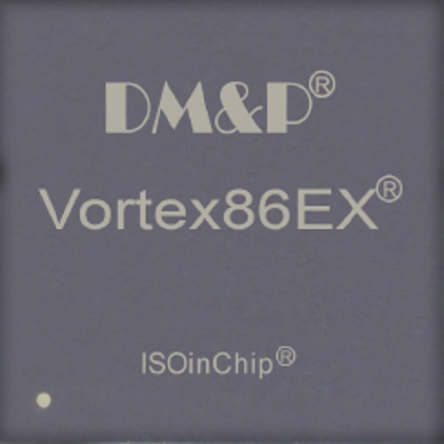
Vortex86EX
The I/O selectable x86 SoC
NEWS
Vortex86 Series Windows Support List
January 08, 2021
NEWS
Vortex86 Series Linux Support List
January 08, 2021
Vortex86EX2
The two independent cores CPU with I/O configurable.
More
Vortex86DX3
The 1GHz dual Core CPU with selectable I/O.
More
Vortex86EX
The I/O configurable CPU.
More