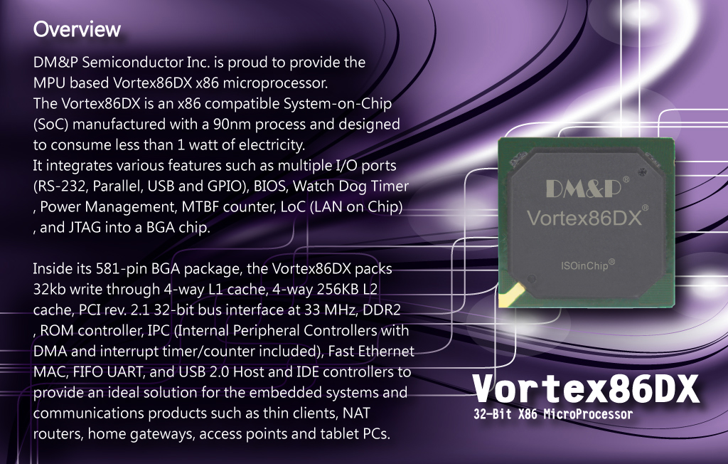
Vortex86DX

The CPU design for industrial application.

Overview

DM&P Semiconductor Inc. is proud to provide the MPU based Vortex86DX x86 microprocessor.

Vortex86DX is an x86 compatible System-on-Chip (SoC) manufactured with a 90nm process and designed to consume less than 1 watt of electricity.
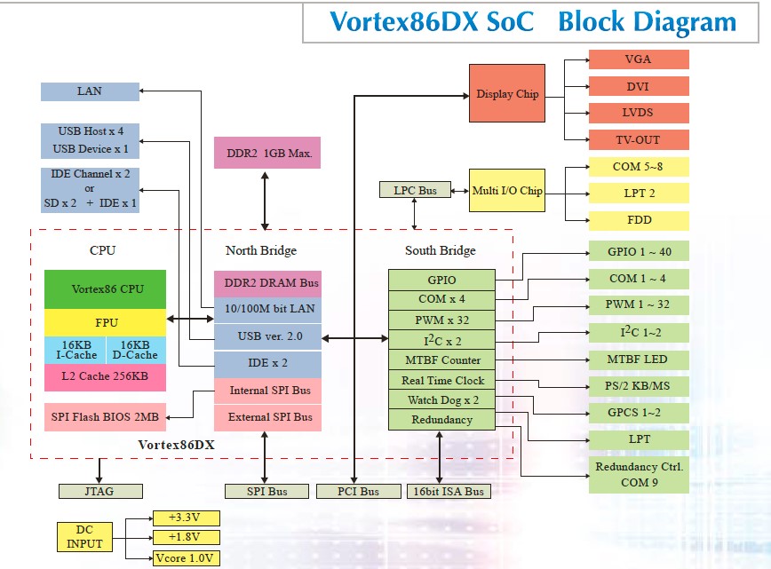
Main Features

  • multiple I/O ports (RS-232, Parallel, USB and GPIO)
  • BIOS
  • Watch Dog Timer
  • Power Management
  • MTBF counter
  • LoC (LAN on Chip)
  • JTAG into a BAG chip

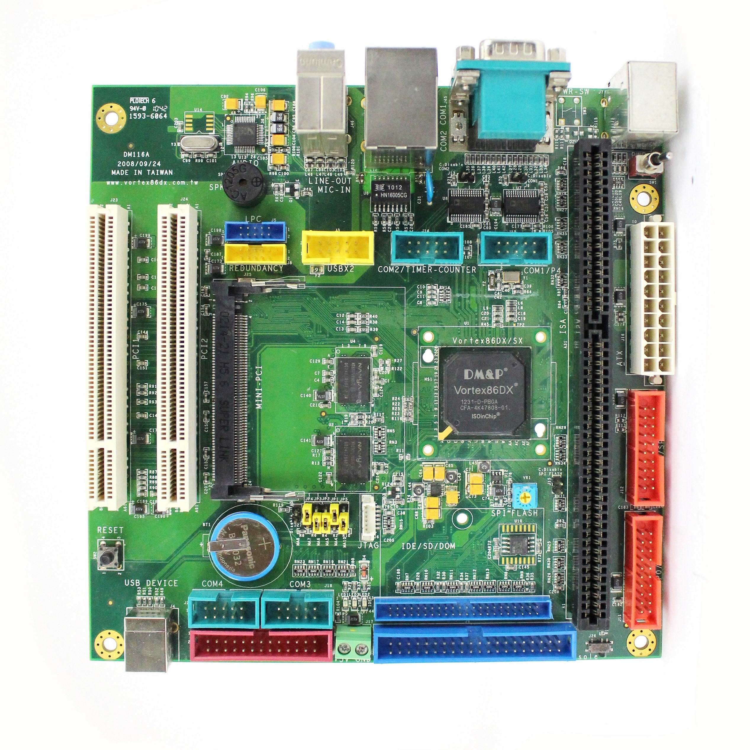
Inside its 581-pin BGA package

  • 32kb write through 4-way L1 cache
  • 4-way 256KB L2 cache
  • PCI rev. 2.1 32-bit bus interface at 33 MHz
  • DDR2
  • ROM controller
  • IPC (Internal Peripheral Controllers with DMA and interrupt timer/counter included)
  • Fast Ethernet MAC
  • FIFO UART
  • USB 2.0 Host and IDE controllers to provide an ideal solution for the embedded systems and communications products

Special Features of Vortex86DX

Integrated MTBF Counter

  • One-time write Flash area for number of MTBF hour before shipment. Timer count up by “hour”. Built-in TTL alert signal will be enabled after time counter over MTBF number. Fault tolerance – Redundancy

Fault tolerance – Redundancy

  • Two CPU boards may be run in parallel—connected to the same ISA bus and executing the same software. Each board will be designated Master or Slave during power on. The system detects six different fail conditions and responds accordingly. I/O can also be switched between boards during each fail over. Contains a built int System Fail Counter.

ISO in Chip

  • 32 Byte one-time write Flash area containing all service tracking data. Data includes: Date codes of all major components, Model and Serial numbers, Unique serial code of SoC, Distributor code, Ship date, etc.

Features of Vortex86DX

x86 32bit Processor Core
  • 6 stage pipe-line
Floating point unit support
Embedded I/D Separated L1 Cache
  • 16K I-Cache
  • 16K D-Cache
Embedded L2 Cache
  • 4-wary 256KB L2 Cache
  • Write through or write back policy
DDRII Control Interface
  • 16 bits data bus
  • DDRII clock support up to 333MHz
  • DDRII size support up to 1GB
IDE Controller
  • Support 2 channels Ultra-DMA 100 (Disk x 4)
  • Primary channel support SD card
LPC (Low Pin Count) Bus Interface
  • Support 2 programmable registers to decode LPC address
MAC Controller x 1
PCI Control Interface
  • Up to 3 sets PCI master device
  • 3.3V I/O
ISA Bus Interface
  • AT clock programmable
  • 8/16 Bit ISA device with Zero-Wait-State
  • Generate refresh signals to ISA interface during DRAM refresh cycle
DMA Controller
Interrupt Controller
Counter/Timers
  • 2 sets of 8254 timer controller
  • Timer output is 5V tolerance I/O on 2nd Timer
MTBF Counter
Real Time Clock (Internal Mode or External Mode)
  • Less than 2uA (3.0V) power consumption in Internal RTC Mode while chip is power-off
FIFO UART Port x 5 (5 sets COM Port)
  • Compatible with 16C550/ 16C552
  • Default internal pull-up
  • Supports the programmable baud rate generator with the data rate from 50 to 460.8Kbps
  • Programmable character options
  • Support TXD_En Signal on COM1/COM2
  • Port 80h output data could be sent to COM1 by software programming
Parallel Port
  • Support SPP/EPP/ECP mode
General Chip Selector
  • 2 sets extended Chip Selector
  • I/O-map or Memory-map could be configurable
  • I/O Addressing: From 2 byte to 64K byte
  • Memory Address: From 512 byte to 4G Byte
General Programmable I/O
  • Supports 40 dedicated programmable I/O pins
  • Each GPIO pin can be individually configured to be an input/output pin
  • GPIO_P0~GPIO_P3 can be programmed by 8051
  • GPIO_P0 and GPIO_P1 with interrupt support (input/output)
USB 2.0 Host Support
  • Supports HS, FS and LS
  • 4 ports
USB 1.1 Host Support
  • Supports FS with 3 programmable endpoints
  • 1 port
PS/2 Keyboard and Mouse Interface Support
  • Compatible with 8042 controllers
Redundant System Support
Speaker out
Embedded 2MB Flash
  • For BIOS storage
  • The Flash could be disable & use external Flash ROM
I²C bus x 2
  • Compliant with V2.1
  • Some master code (general call, START and CBUS) not support
Servo Control interface support
General Shift interface support
JTAG Interface supported for S.W.
debugging
Input clock
  • 14.318MHz
  • 32.768KHz
Output clock
  • 24 MHz
  • 25 MHz
  • PCI clock
  • ISA clock
  • DDRII clock
Operating Voltage Range
  • Core voltage: 1.2 V ~ 1.4V
  • I/O voltage: 1.8V ± 5%, 3.3 V ± 10 %
Operating temperature
  • -40°C ~ 85°C
Package Type
  • 27x27mm
  • 581 ball BGA

System Block Diagram

VDX-6390

For detail reference design, schematic, gerber, layout, layout guide ....etc, please contact soc@dmp.com.tw to get the FTP access for all the reference design documents.

Vortex86DX support most of legacy OS and RTOS which provide standard x86 BSP. Please contact soc@dmp.com.tw if you can't download proper information or driver from our website. 


Windows: CE 6.0, Embedded Compact 7

Linux : Up to kernel 4.14 with QT support, the Buildroot step by step guide is also available.

Other OS Support: For QNX, VxWorks and RTOS 32 support, please contactsoc@dmp.com.tw

Our Life Cycle Policy:

All of DMP Electronics product should have at least 10 years life cycle. For detailed information, please contact soc@dmp.com.tw.