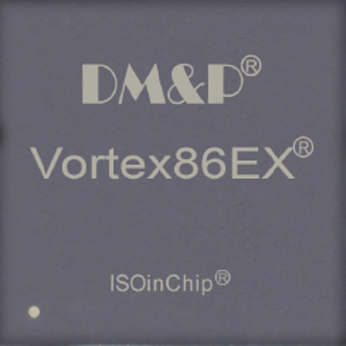
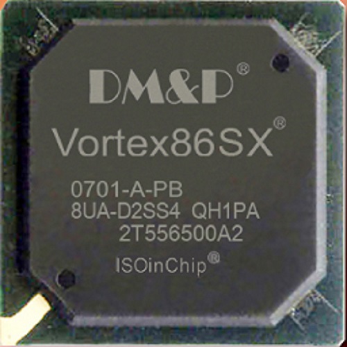
Vortex86SX

The first SoC with build-in North & South Bridge.

Overview

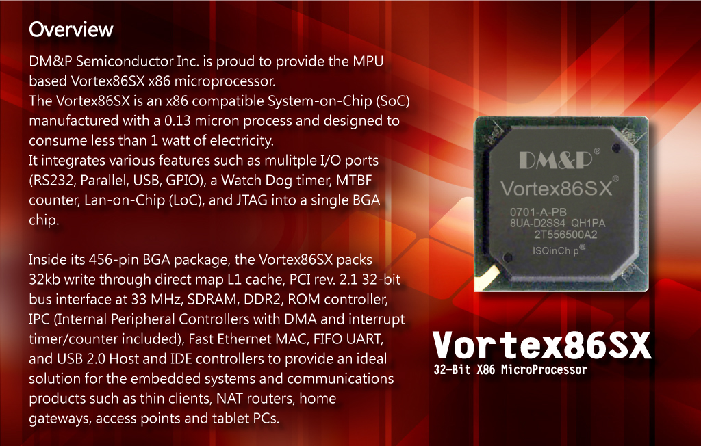
DM&P Semiconductor Inc. is proud to provide the MPU based Vortex86SX x86 microprocessor. 
Vortex86SX is an x86 compatible System-on-Chip (SoC) manufactured with a 0.13-micron process and designed to consume less than 1 watt of electricity.

Main Features

  • multiple I/O ports (RS232, Parallel, USB, GPIO)
  • a JTAG into a single BGA chip

Inside its 456-pin BGA package

  • 32kb write through direct map L1 cache
  • PCI rev. 2.1 32-bit bus interface at 33 MHz
  • SDRAM
  • DDR2
  • ROM controller
  • IPC (Internal Peripheral Controllers with DMA and interrupt timer/counter included)
  • Fast Ethernet MAC
  • FIFO UART
  • USB 2.0 Host
  • IDE controllers to provide an ideal solution for the embedded systems and communications products
Features of Vortex86SX

x86 32bit Processor Core
  • 6 stage pipe-line
Embedded I/D Separated L1 Cache
  • 16K I-Cache
  • 16K D-Cache
SDRAM/DDRII Control Interface
  • Support DLL for clock phase auto-adjust
IDE Controller
  • Support 2 channels Ultra-DMA 100 (Disk x 4)
LPC (Low Pin Count) Bus Interface
  • Support 2 programmable registers to decode LPC address
MAC Controller x 1
PCI Control Interface
  • Up to 3 sets PCI master device
  • 3.3V I/O
ISA Bus Interface
  • AT clock programmable
  • 8/16 Bit ISA device with Zero-Wait-State
  • Generate refresh signals to ISA interface during DRAM refresh cycle
DMA Controller
Interrupt Controller
Counter/Timers
  • 2 sets of 8254 timer controller
  • Timer output is 5V tolerance I/O on 2nd Timer
Real Time Clock (Internal Mode or External Mode)
  • Below 2uA power consumption on Internal Mode (Estimated Value)
FIFO UART Port x 5 (5 sets COM Port)
  • Compatible with 16C550/ 16C552
  • Default internal pull-up
  • Supports the programmable baud rate generator with the data rate from 50 to115.2Kbps
  • The character options are programmable for 1 start bits; 1, 1.5 or 2 stop bits; even, odd or no parity; 5~8 data bits
  • Support TXD_En Signal on COM1/COM2
  • Port 80h output data could be sent to COM1 by software programming
General Chip Selector
  • 2 sets extended Chip Selector
  • I/O-map or Memory-map could be configurable
  • I/O Addressing: From 2 byte to 64K byte
  • Memory Address: From 512 byte to 4G Byte
General Programmable I/O
  • Supports 40 dedicated programmable I/O pins
  • Each GPIO pin can be individually configured to be an input/output pin
USB 2.0 Host Support
  • Supports HS, FS and LS
  • 4 ports
PS/2 Keyboard and Mouse Interface Support
  • Compatible with 8042 controller
Speaker out
Embedded 256KB Flash
  • JTAG Interface supported for S.W. debugging
Input clock
  • 14.318MHz
  • 32.768KHz
Output clock
  • 24 MHz
  • 25 MHz
Operating Voltage Range
  • Core voltage: 1.2 V ~ 1.4V
  • I/O voltage: 1.8V ± 5%, 3.3 V ± 10 %
Operating temperature
  • -40℃ ~ 85℃
Package Type
  • 27x27mm
  • 456 ball BGA

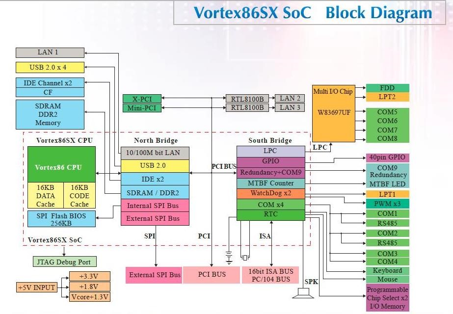
System Block Diagram

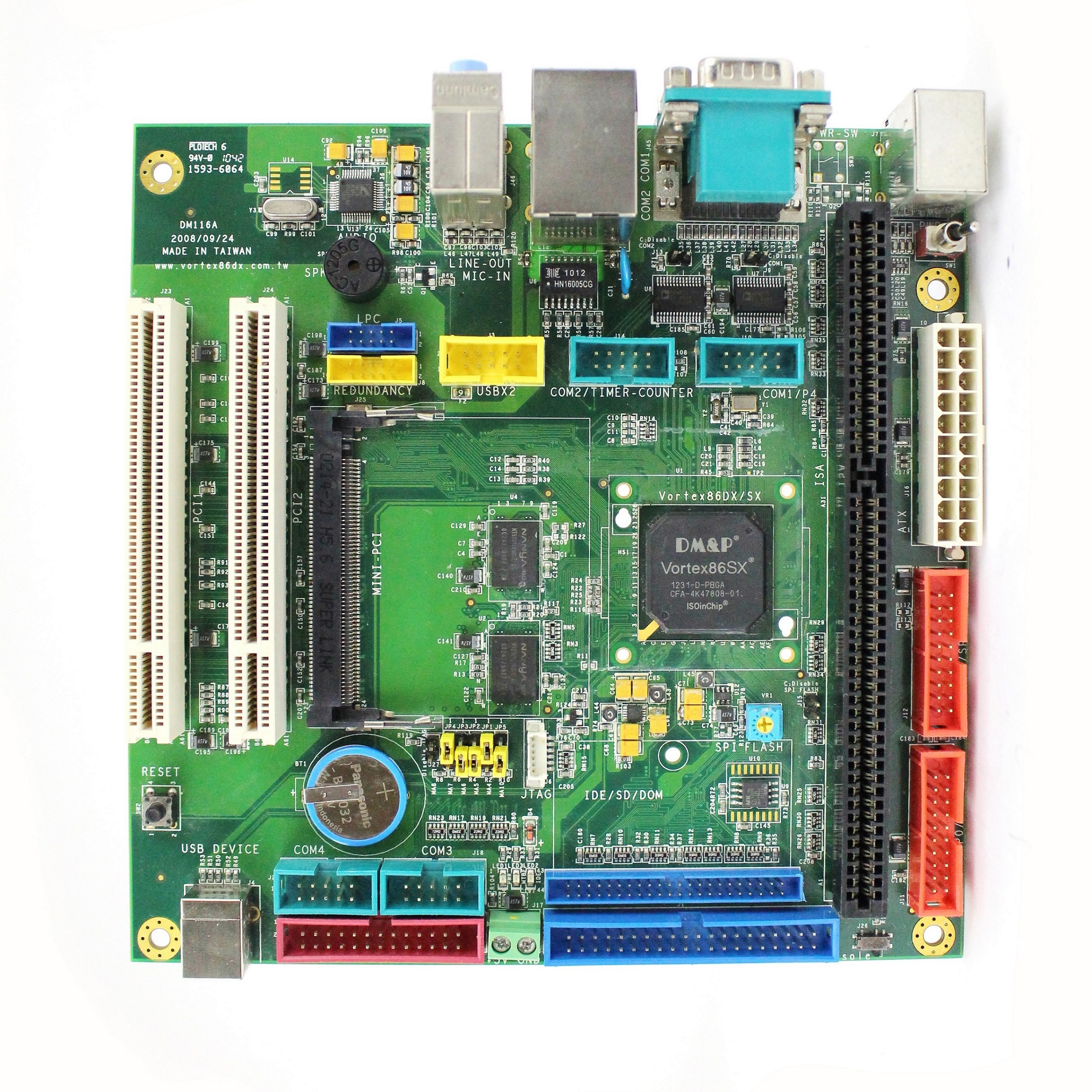
VSX-6190

For detail reference design, schematic, gerber, layout, layout guide ....etc, please contact soc@dmp.com.tw to get the FTP access for all the reference design documents.

Vortex86SX support most of legacy OS and RTOS which provide standard x86 BSP. Please contact soc@dmp.com.tw if you can't download proper information or driver from our website. 


Windows: CE 6.0, Embedded Compact 7

Linux : Up to kernel 4.14 with QT support, the Buildroot step by step guide is also available.

Other OS Support: For QNX, VxWorks and RTOS 32 support, please contactsoc@dmp.com.tw

Our Life Cycle Policy:

All of DMP Electronics product should have at least 10 years life cycle. For detailed information, please contact soc@dmp.com.tw.